How much silicon does it take to add an AV1 decoder to a chip? The areas Apple highlighted in their A17 release looked pretty substantial, but I wasnt sure if it was to scale.
I'm pretty sure that a video codec ASIC would share some building blocks across codecs, with per-codec parameterization, so I don't think Apple literally added a single "AV1 box" to the A17/M3 die.
I'm sure the usual suspects (Synopsys, Broadcom, ARM, Xilinx, etc.) would be happy to license something. But from what I can see all the big players make their own. I guess they're easy enough to implement yourself (as a big player) and important enough to not want to leave it in the hands of a third party.
There are also likely opportunities for additional efficiencies when you make a custom {en,de}coder for your system. I suspect (but haven't confirmed) that the typical Intel/AMD/Nvidia/Apple multi-function media engine isn't just a collection of completely independent encoder/decoder blocks for each codec but a kind of simplified specialized microcoded CPU with a collection of fixed-function blocks which can be shared between different codecs. So it could have blocks that do RGB->YUV conversion, Discrete Cosine Transforms, etc. and you can use the same DCT block for AV1, HEVC, and AVC. Maybe you can also create specialized efficient ways to transfer frames back and forth with the GPU, for sharing cache with the GPU, etc.
My understanding (now several years out of date) is that Arm decided not to pursue licensing a design, because every customer they talked to had requirements that were so different that they would have essentially been one-offs that each required significant additional engineering. I cannot speak to the others you mention.
I believe the team we worked with at Arm during AV1 standardization is no longer there, which is too bad. They were really great guys to work with.
Your suspicion is mostly correct, though obviously you cannot share too much of the DCTs as these must be bit-exact and are different for each of the standards. But especially things like the compressed tile cache for reference frames used in motion compensation are extremely complicated (to save memory bandwidth and power) and entirely shareable. The SRAM used for line buffers is also a lot of area and shareable. And so on.
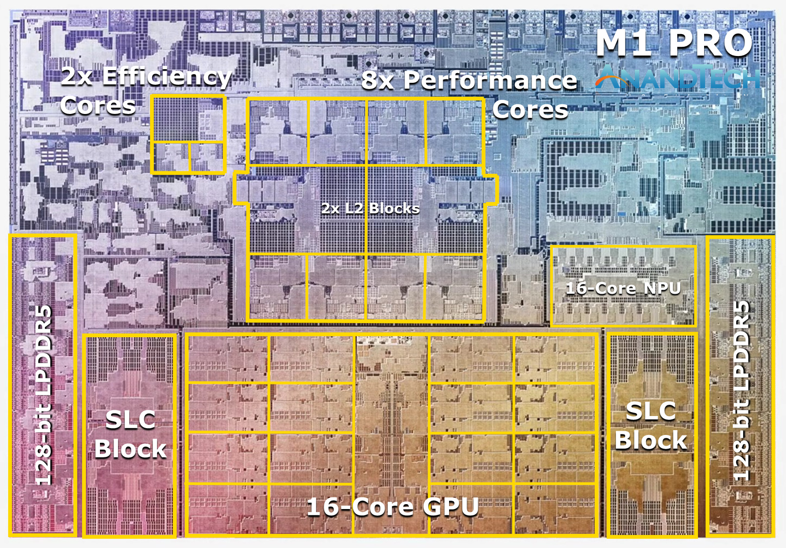
It is a pure marketing slide. The M3 variants floorplans don't look anything like that, as can be seen on other pictures of the dies.
That being said, it's pretty common to have dedicated silicon for video codecs. It normally takes the form of a little DSP with custom instructions to accelerate operations specific to the codec.
I agree that is how I'd expect it to be implemented, but I'm not sure how small it would be given the processing bandwidth we are talking about for 4k video.
I'm guessing this is a distinct region of the chip and not integrated with CPU/GPU since they scale up by replicating those blocks and wouldn't want to redundantly place that hardware. Having it separate also allows a team to work on it independently.
I think the relative size of the media engines is accurate in that slide, so then it comes down to how large the ProRes parts are in other chips. They are probably a couple of the unlabeled regions next to the performance cores in the M1 Pro die shot below, but I don't know which.
A GPU is also not a monolith. As you say, there are some functions that scale with the number of compute units, but others don't need to (e.g. display scan-out controllers); it would accordingly make sense to make the video coding functions part of the latter.
And video decoding/encoding is definitely at least GPU-adjacent, since it usually also involves scaling, color space transformations etc.
I've seen it. Sometimes because the DSP is hyperspecialized for a particular codec. Sometimes just because the SoC vendor bought the hard codecs from different sub vendors.
You can either have a fully dedicated core for codecs, or you can just put certain codec related operations (like DCT-related SIMD) in your main cores. Cryptographic acceleration tends to use the latter approach.
Video codecs usually come with GPUs, not CPUs. It is only on SoCs where this distinction is a more fuzzy.
On a GPU, you didn't have an option to interleave normal program stream with specialized partial-decoding instruction. You put encoded frame in and you get decoded frame back, the media engine was separate block from compute.
Though this is also changing; see Intel GuC firmware, which has (optionally) some decoding, encoding and processing based on compute.
https://b3148424.smushcdn.com/3148424/wp-content/uploads/202...